How to draw a circuit board at home. We make a printed circuit board with a marker. Etching solution based on hydrogen peroxide and hydrochloric acid
Let's look at the process of making printed circuit boards at home using a specific example. You need to make two boards. One is an adapter from one type of case to another. The second is replacing a large microcircuit with a BGA package with two smaller ones, with TO-252 packages, with three resistors. Board sizes: 10x10 and 15x15 mm. There are several options for making printed circuit boards at home. The most popular ones are using photoresist and “iron-laser technology”.
Instructions for making printed circuit boards at home
You will need
- personal computer with a program for tracing printed circuit boards;
- laser printer;
- thick paper;
- fiberglass;
- iron;
- hacksaw;
- acid for etching the board.
1 Project preparation printed circuit board
We are preparing a project printed circuit board. I use the DipTrace program: convenient, fast, high quality. Developed by our compatriots. Very convenient and pleasant user interface, unlike the generally accepted PCAD. Free for small projects. Libraries of electronic components housings, including 3D models. There is a conversion to PCAD PCB format. Many domestic firms have already begun to accept projects in the DipTrace format.
PCB design
The DipTrace program allows you to see your future creation in volume, which is convenient and visual. This is what I should get (the boards are shown in different scales):

2 Marking fiberglass laminate
First, we mark the PCB and cut out the blank for the printed circuit boards.

3 Project output on a laser printer
We output the project on a laser printer in a mirror image in the highest possible quality, without skimping on toner. After much experimentation, the best paper for this was chosen - thick matte printer paper. You can try using photo paper or buy special thermal paper.

4 Transferring a project for fiberglass
Let's clean and degrease the board blank. If you don’t have a degreaser, you can go over the copper foil of fiberglass with a regular eraser. Next, using an iron, we “weld” the toner from the paper to the future printed circuit board. I hold it for 3-4 minutes under slight pressure until the paper turns slightly yellow. I set the heat to maximum. I put another sheet of paper on top for more even heating, otherwise the image may “float”.
The important point here is the uniformity of heating and pressure and heating time. If you don't hold the iron down enough, the print will be washed off during etching, and the tracks will be corroded by acid. If you overexpose it, nearby conductors may merge with each other.

5 Removing the paper from the workpiece
After this, we place the workpiece with the paper stuck to it in the water. You don’t have to wait for the textolite to cool down. Photo paper quickly gets wet, and after a minute or two you can carefully remove the top layer.

In places where there is a large concentration of our future conductive paths, the paper sticks to the board especially strongly. We're not touching it yet. Let the board soak for a couple more minutes. Now the remaining paper is removed using an eraser or rubbing with your finger. You should end up with a beautiful, clean piece with a clearly printed design.
 Removing the remaining paper from the printed circuit board blank
 6 Preparing the board to etching
We take out the workpiece. Dry it. If somewhere the tracks are not very clear, you can make them brighter with a thin CD marker or nail polish, for example (depending on what you are going to etch the board with).

It is necessary to ensure that all the paths come out clear, even and bright. It depends on the:
- uniformity and sufficiency of heating the workpiece with an iron;
- be careful when removing paper;
- quality of PCB surface preparation;
- good selection of paper.
Experiment with different types paper, at different times heating, different types of fiberglass surface cleaning to find the most optimal quality option. By choosing an acceptable combination of these conditions, in the future you will be able to produce printed circuit boards at home faster and with better quality.
7 Etching printed circuit board
We place the resulting workpiece with future conductor tracks printed on it in an acid, for example, in a solution of ferric chloride. We'll talk about other types of etching later. We poison for 1.5 or 2 hours. While we wait, cover the bath with a lid: the fumes are quite caustic and toxic.

8 Flushing printed circuit board
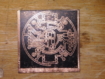
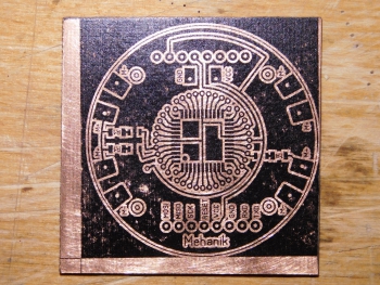
We take the finished boards out of the solution, wash and dry. Toner from a laser printer can be easily washed off the board using acetone. As you can see, even the thinnest conductors with a width of more than 0.2 mm came out quite well. There is very little left.

8 Tinning printed circuit board
We tin the manufactured printed circuit boards. We wash off the remaining flux with gasoline or an alcohol-gasoline mixture.
All that remains is to cut out the boards and mount the radio elements!
conclusions
With a certain skill, the “laser-iron method” is suitable for making simple printed circuit boards at home. Conductors from 0.2 mm and thicker are clearly obtained. Time for preparation, experiments with selecting the type of paper and iron temperature, etching and tinning takes approximately 2 to 5 hours. When will you find optimal combination, the time spent on making the board will be less than 2 hours. This is much faster than ordering boards from a company. Cash costs are also minimal. In general, for simple budget amateur radio projects, the method is recommended for use.
Hello, dear blog readers. The weather is wonderful outside now, and I have great mood. Today I want to tell you about how you can make high-quality printed circuit boards at home.
]In general, the method of manufacturing printed circuit boards using laser iron not complicated. Its essence lies in the method of applying a protective pattern to foil PCB.
In our case, we first print the protective design using a printer onto photo paper, its glossy side. Then, as a result of heating with an iron, the softened toner is fried to the surface of the PCB. Read on for details of this action... BUT in the following articles you will find even more helpful information from the field of amateur radio technology so be sure to subscribe.
So let's get started.
To make a board using LUT technology we will need:
- foil textolite (single- or double-sided)
- laser printer
- metal scissors
- glossy photo paper (Lomond)
- solvent (acetone, alcohol, gasoline, etc.)
- sandpaper (fine abrasive, zero grit is fine)
- drill (usually a motor with a collet chuck)
- toothbrush (very necessary thing, not only for dental health)
- ferric chloride
- actually the board drawing itself was drawn in Sprint-Layout
Preparation of textolite
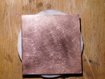
We take metal scissors in our hands and cut out a piece of PCB to the size of our future printed circuit board. Previously, I cut PCB with a hacksaw for metal, but it turned out that it was not so convenient compared to scissors, and the PCB dust was very annoying.
We thoroughly sand the resulting printed circuit board blank with sandpaper - zero grade until a uniform mirror shine appears. Then we moisten a piece of cloth with acetone, alcohol or some other solvent, thoroughly wipe and degrease our board.
Our task is to clean our board from oxides and “sweaty hands”. Of course, after this we try not to touch our board with our hands.
Preparing a printed circuit board design and transferring it to textolite
We print the pre-drawn design of the printed circuit board onto photo paper. Moreover, we turn off the toner saving mode in the printer, and display the drawing on the glossy side of the photo paper.

Now we take the iron out from under the table and plug it in, let it heat up. We place a freshly printed sheet of paper on the textolite with the pattern down and begin to iron it with an iron. With photographic paper, unlike tracing paper or self-adhesive backing, there is no need to stand on ceremony; simply iron it until the paper begins to yellow.
Here you don’t have to be afraid to overexpose the board or overdo it with pressure. Afterwards we take this sandwich with fried paper and take it to the bathroom. Using your fingertips, begin to roll up the paper under running warm water. Next, we take the prepared toothbrush in our hands and carefully pass it over the surface of the board. Our task is to tear off the white chalky layer from the surface of the drawing.

We dry the board and check it thoroughly under a bright lamp.
Often the chalky layer is removed the first time with a toothbrush, but it happens that this is not enough. In this case, you can use electrical tape. The whitish fibers stick to the electrical tape, leaving our scarf clean.
Board etching
To prepare the etching solution we need ferric chloride FeCL3.

This miracle powder in our radio store costs about 50 rubles. Pour water into a non-metallic container and add ferric chloride into it. Usually take one part FeCL3 to three parts water. Next, we immerse our board in the vessel and give it time.
The etching time depends on the thickness of the foil, the temperature of the water, and the freshness of the prepared solution. The hotter the solution, the faster the etching process will take place, but at the same time hot water there is a possibility of damage to the protective pattern. Also, the etching process is accelerated by stirring the solution.

Some people use a “bulbulator” from an aquarium for this purpose, or attach a vibration motor from a telephone. We take out the etched board and rinse it under running water. We pour the etching solution into a jar and hide it under the bathtub, the main thing is that the wife does not see it.
This solution will be useful to us later. We clean the etched scarf from the protective layer of toner. I use acetone for this, but it seems that alcohol or gasoline also works well.

Drilling the board
The etched and cleaned board requires drilling, since it is not always possible to use surface mounting. I have a small drill bit for drilling the board. It is a DPM type motor with a collet chuck mounted on the shaft. I bought it at a radio store for 500 rubles. But I think you can use any other motor for this, for example from a tape recorder.

We drill the board with a sharp drill, trying to maintain perpendicularity. Squareness is especially important when making double-sided boards. We do not need to punch holes for drilling, since the holes in the foil were formed automatically during etching.
We go over the board with sandpaper, removing burrs after drilling, and get ready to tinning our board.
Tinning boards
I try to tin my boards, and I do this for several reasons:
- A tinned board is more resistant to corrosion, and after a year you will not see any traces of rust on your device.
- The solder layer on the printed pattern increases the thickness of the conductive layer, thereby reducing the conductor resistance.
- It is easier to solder radio components onto a pre-tinned board; prepared surfaces facilitate high-quality soldering.
We degrease the board and clean it of oxide. Let's use acetone, and then literally dip it in a solution of ferric chloride for a second. We paint the pinkish board generously with flux. Next, we take out a more powerful soldering iron and, having collected a small amount of solder on the tip, quickly move along the paths of our printed design. All that remains is to go over the design a little with sandpaper, and as a result we get a beautiful, shiny scarf.

Where can I buy
Where can you buy foil-coated PCB? Yes, by the way, not only textolite, but also other tools for amateur radio creativity.
Currently, I don’t have any problems with this, since there are several decent radio stores in my city. There I buy textolite and everything I need.
At one time, when there was no normal radio store in my city, I ordered all the materials, tools and radio parts from the online store. One of these online stores where you can find textolite and not only this is the Dessie store, by the way, I’m even talking about it.
Custom printed circuit boards
There are situations when there is a drawing of a printed circuit board, but you absolutely don’t want to deal with technological problems and the printed circuit board is so necessary. Or it happens that you don’t mind trying, comprehending all the mysteries of this process, but there is no time for evil and you don’t know what it will lead to (the first result is not always close to ideal) In this case, you can do it easier, you can get a high-quality result.
So ATTENTION!!!
If you are interested in making custom printed circuit boards, be sure to read! Well, so we got acquainted with the method of making printed circuit boards with our own hands at home. Necessarily subscribe to new articles
, because there will be a lot of interesting and useful things to come. In addition, relatively recently another progressive method of subscription has appeared through the form of the Email newsletter service. This method is notable for the fact that Every subscriber receives a GIFT!!!
, and this gift will undoubtedly be appreciated by any radio amateur. So people sign up and get nice bonuses, so you're welcome. So create your devices, make printed circuit boards , A LUT technology
will help you.
Best regards, Vladimir Vasiliev. I suggest you look good selection
videos on each stage of LUT technology.
Technology for manufacturing printed circuit boards at home
"...and experience is the son of difficult mistakes..." So, the board manufacturing process begins with schematic diagram future device. At this stage, you determine not only how the components will be connected to each other, but also decide which components are suitable for your design. For example: use standard parts or SMD (which, by the way, also come various sizes
). The size of the future board will depend on this. Next, we decide on the choice software , with which you will draw the future board. While a circuit diagram can be drawn by hand, this cannot be done with a printed circuit board design (especially when it comes to SMD components). I use . I downloaded it a long time ago and have been using it. Very good program
Haven't discovered any secrets yet? So: when the board drawing has already been created, you have made sure that the components are located correctly, you should set the “ground”, i.e. fill the gaps between the tracks and holes; for this purpose, the program has a special function that does this automatically (by default the gap is 0.4 mm). Why is this necessary? So that etching (we'll look at it later) takes less time, it will be easier for you to control the process and it is also useful to do this for circuit design reasons...

Note: When designing a board, try not to make holes smaller than 0.5 mm in diameter, unless, of course, you have a special machine for drilling holes, but more on that later...
Great! We have drawn a drawing of the future printed circuit board, now it needs to be printed on a LASER printer (Lut means laser). To do this, click print. The above-mentioned program creates a special file, in which you can select the number of copies, their location, make a frame, specify the size of the holes and mirror.
Note: if you are making a double-sided PCB, then front part it is necessary to reflect horizontally, and leave the wrong side as is. ConcerningSprint- Layout, then it is better to do this at the stage of creating the diagram, and not at the stage of preparing the file for printing, since “glitches” arise with the “mass”, it disappears in some places.
And yet, it is better to print several copies, even if you only need one copy, because defects may appear in the next stages and in order not to run to the printer every time, do this in advance.
What to print on? To begin, print it out on a regular sheet of paper so that last time make sure that everything is done correctly and that all components fit in size. This will also warm up the printer.

Now we set the maximum toner density, disable all saving modes (by the way, it is better to use a fresh cartridge). We take a backing of self-adhesive paper, preferably “velvet” paper (the best result is obtained with it, maybe this is due to the fact that it is thicker), insert it with the shiny side into the printer and press “print”. Ready!

Note: from now on, you cannot touch this paper, only by the edges, otherwise you may stain the drawing!
About reusing the substrate. Let's say that you printed out a drawing, but it only took up half of the sheet, you don't need to throw away the other half, you can print on it too, BUT! for some reason, when printing again, the printer “chews” the paper in 20% of cases, so be careful!
Preparing textolite
I use regular foil fiberglass laminate 1 mm thick, which is sold in a radio parts store. Since we want to make a double-sided board, we buy double-sided PCB. We cut off the required piece, there is no need to make a reserve, it will not be needed. They cut it off. We take zero sandpaper and sand the textolite until shiny on both sides. If there are small scratches, then it’s okay, the toner will stick better (but without fanaticism!). Next, take acetone (alcohol) and wipe the board on both sides to degrease it. Ready!

Note: when you sand the PCB, pay attention to the corners of the board, very often they are “under-sanded” or, even worse, “over-sanded”, this is when there is no foil left there at all. After wiping with acetone, the board should also not be touched with your hands; you can only grab it by the edges, preferably with tweezers.

Next is the most important stage: transferring the design from paper to textolite. It is done using an iron (lut means iron). Anyone will do here. We heat it to 200 degrees (often this is the maximum temperature of the iron, so we just turn the regulator to maximum and wait for it to heat up).
And now here are the secrets! To transfer a printed circuit board design from paper to PCB, you need to attach the paper to the PCB with the desired side, then press it with an iron and smooth it out thoroughly. Doesn't seem complicated? But the most difficult thing is to apply the iron so as not to sweep away the paper, especially if the scarf is small and you are making it in a single copy; besides, it is not so easy to use the iron. Eat interesting way make the task easier.
Note: We're looking at making double-sided PCBs, so a little about paper preparation. Some sources advise doing this: transfer one side, seal the opposite side with tape or tape, etch one side, then drill holes, match the pattern of the other side, then transfer it again, seal it, etch. This takes a lot of time because you essentially have to etch two boards! You can speed up the process.
We take two pieces of paper with a design on the front and back sides and combine them. This is best done on a glass window or on a transparent table with lighting. Note! in this case, it is necessary to cut off the pieces of paper with a margin, the more the better, but without fanaticism, 1-1.5 cm is enough. We fasten them with a stapler on 3 sides (no glue!), We get an envelope in which we put the board and align it.

The most interesting. We take two pieces of PCB (see the size in the figure), place them with the foil side facing each other, and between them we place an “envelope” with a board, and secure the edges of this sandwich with paper clips so that the PCB sheets do not move relative to each other.

Note: for these purposes, it is better to choose a thinner textolite; it will warm up faster and will be able to deform where necessary.

Now, we take the iron and calmly apply it to our sandwich, and press as hard as we can, first on one side, then turn it over and press on the other. For the best effect, I recommend that after the first pressure, make several circular movements with the iron to be sure that the paper is pressed in all places. You don't need to iron for long, usually no more than 1-3 minutes for everything, but no one will tell you the exact time, because it depends on the size of the board and the amount of toner. The main thing is not to overexpose, because in this case the toner may simply spread, and if you underexpose, the drawing may not be completely transferred. Practice, gentlemen, practice!
Then you can open the sandwich and make sure that the paper is stuck to the PCB on all sides, i.e. no air bubbles. And we quickly carry the board under running water and cool it ( cold water of course).
Note: If you used a backing from self-adhesive paper, then it will fall off the PCB itself under water and the board will easily fall out of the envelope. If you used a velvet paper backing (thicker), then this will not work with it. We take scissors and cut off the sides of the envelope, then slowly, holding the edge of the paper, remove the paper under running water. As a result, there should be no toner left on the paper; it will all be on the PCB.
At this stage, if defects occur, there are two ways to proceed. If there are too many defects, it is better to take acetone, wash off the toner from the PCB and try again (after first repeating the process of cleaning the PCB with sandpaper).
An example of an irreparable defect (in this case, I started over):


If there are few defects, then you can take a marker for drawing printed circuit boards and fill in the defects.
A good option, there are small holes in the “mass”, but they can be painted over with a marker:
Corrected options. The green shaded areas are clearly visible:


Great, this was the most technologically difficult stage, it will be easier later.
Now you can etch the board, i.e. remove excess foil from the PCB. The essence of etching is this: we place the board in a solution that corrodes the metal, while the metal located under the toner (under the board pattern) remains unharmed, and the one around it is removed.
I'll say a few words about the solution. In my opinion, it is better to poison with ferric chloride, it is not expensive, the solution is very easy to prepare, and overall it gives a good result. The recipe is simple: 1 part ferric chloride, 3 parts water and that’s it! But there are other methods of etching.
Note: you need to add water to the iron, and not vice versa, that’s how it should be!
Note: There are two types of ferric chloride (that I have seen): anhydrous and 6-hydrous. Anhydrous, as the name implies, is completely dry, and there is always a lot of dust in the container in which it is sold, this is not a problem. But when water is added, they will actively dissolve, a strong exothermic reaction occurs (the solution heats up), with the release of some kind of gas (most likely it is chlorine or hydrogen chloride, well, it’s a rare dirty trick), which CANNOT BE INHALED, I recommend diluting it in air.
But 6-water iron is already better. This is, in fact, already a solution, water is added, wet lumps are obtained, which also need to be added to the water, but there is no such violent reaction anymore, the solution heats up, but not very quickly and not very much, but everything is safe and quiet (windows are still needed open).

Note: the advice that I give here is not the only correct one; on many forums you can meet people who have obtained boards with a different concentration, a different type of ferric chloride, etc. I just tried to summarize the most popular tips and personal experience. So, if these methods did not help, then try another method and you will succeed!
Have you prepared the solution? Great! Select a container. For single-sided ones, this choice is simple, we take a transparent (to see the etching process) plastic box with a lid, put the board on the bottom. But with double-sided boards it's not so simple. It is necessary that the etching speed on each side be approximately the same, otherwise a situation may arise where one side has not yet been etched, but the tracks on the other are already dissolving. To prevent this from happening, you need to place the board vertically in the container (so that it does not lie on the bottom), then the solution around will be homogeneous and the etching rate will be approximately the same. Therefore, it is necessary to take a high capacity so that the board fits into the " full height"It is better to choose a narrow transparent jar so that you can observe the etching process.


Next, the solution must be heated (we place it on the battery), this will increase the speed of the reaction, and shake periodically to ensure uniform etching and to avoid the appearance of sediment on the board.
Note: some people put it in the microwave and heat it there, but I don’t recommend you do this, because... I read on one forum that after this you can get poisoned by food from this microwave. There is no direct evidence, but it’s better not to risk it!
Note: to ensure uniform etching, you need to stir the solution (shake the container), but there are more technological methods. You can attach a bubble generator (from an aquarium) to the container and then the bubbles will mix the solution. I've seen people making oscillating etching pots with a servo motor and a microcontroller that does the "shaking" according to a special algorithm! Here I do not consider each option in detail, because each has its own nuances and the article would then be very long. I described the simplest method, which is perfect for the first boards.
We are waiting, no need to rush!
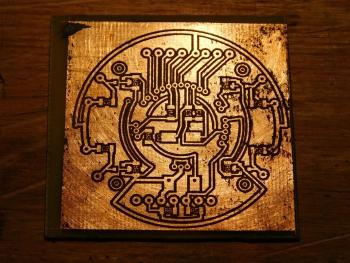
It is very easy to understand that the etching process has ended: there will be no traces of foil between the black toner. When this happens, you can remove the board.
Next, we carry it under water and wash off the remaining solution. Take alcohol or acetone and wash off the toner; there should be foil tracks underneath it. Great, is everything okay? Are there any “under-etched” places? Are there any “over-etched” places anywhere? Great! We can move on!

Note: if defects appear at this stage of production, you are faced with a serious choice: throw away the defect and start over, or try to fix it. It depends on how serious the defects are and how high your demands are on your work.
The next stage is tinning the board. There are two main ways. The first one is the simplest. We take soldering flux (I use LTI-120, but not the one that looks like rosin varnish, which leaves terrible stains on the soldering field, but the alcohol-based one, it is much lighter), generously lubricate the board with it on one side. We take solder and a soldering iron with a wide tip and begin to tin the board, i.e. Cover the entire foil with solder.

Note: do not keep the soldering iron on the tracks for too long, because... Textolite comes in different qualities and some of the tracks fall off very easily, especially thin ones. Be careful!
In this case, solder streaks or unpleasant-looking bumps may appear on the board; it is better to deal with them using a desoldering braid. In those places where it is necessary to remove excess solder, we apply it, all excess solder is removed and a flat surface remains.
Note: you can immediately wrap the braid around the tip and tin with it right away, this may turn out even easier.


The method is good, but to achieve an aesthetically pleasing appearance of the board, some experience and skill is required.
The second method is more complicated. You'll need metal container, in which you can boil water. Pour water into a container, add a couple of spoons citric acid and put on gas, bring to a boil. The solder should not be simple, but one with a low melting point, for example Rose alloy (about 100 degrees Celsius). We throw a few balls to the bottom and see that they have melted. Now we throw the board onto these balls, then take a stick (preferably a wooden one, so as not to burn your hands), wrap it in cotton wool and begin to rub the board, disperse the solder along the tracks, thus achieving an even distribution of solder throughout the board.
The method is quite good, but more expensive, and you need to choose a container, because you will have to use tools in it. It is better to use something with low sides.
Note: you will have to do this operation for quite a long time, so it is better to open the window. With experience you should get faster.
Note: many do not speak very well of Rose alloy due to its fragility, but it is very suitable for tinning boards using this method.
Note: I myself don’t like this method, because I tried to use it when I made the first board and I remember well how inconvenient it was to “cook” this board in tin can without tools....Oh that was terrible! But now...
Both methods have their advantages and disadvantages; the choice depends only on you and your capabilities, desires, and skills.
Note: I further recommend testing the board with a multimeter to make sure that there are no intersections of tracks that should not intersect, that there are no random “nozzles” or any other surprise. If we find a problem, take a soldering iron and remove the excess solder; if that doesn’t help, then use a utility knife and carefully separate the necessary places. This may mean that the board is under-etched in some places, but that's okay.
To do this we use a small drill and a drill bit. Now on sale special drills for printed circuit boards with special sharpening and special grooves on the drill. First I used regular drill on metal 0.6 mm thick, then switched to a special one and the result is very good. Firstly, even with my budget drill, any PCB can be drilled without any problems, with almost no effort. The drill itself “bites” into it and pulls the tool along with it. Secondly, it leaves a neat entry and exit hole, without burrs, unlike a standard drill, which literally “tears” the PCB. Thirdly, this drill almost does not slip, i.e. You just need to get to the right place the first time and it won’t go anywhere. A miracle, not a tool! But it also costs a little more than a regular drill.
Note: to “get to the right place right away” it is better to use an awl or a special tool for punching, just do not make too deep cuts, this may direct the drill in the wrong direction. Also: this drill has one drawback - it breaks easily, so it is better to use a special machine to drill holes or hold the drill strictly vertically. Believe me, it breaks very easily! Especially when you need to drill a hole of 0.3 mm or 0.2 mm, but this is already jewelry work.
Ready! That's all! We solder the through holes with thin wires and we get neat hemispheres on the board, it looks very nice. Now you just need to solder all the components of the circuit and make sure that it works, but this is a topic for another article. And here's what I got:


That's all. Once again I want to emphasize that here I only tried to summarize all the materials that I managed to find about LUT, and my experience. It turned out a little long, but in every case there are many nuances that must be taken into account to achieve the best result. The last piece of advice I can give you is: you need to try, try to make boards, because mastery comes with experience. And at the end I will once again quote the epigraph: “...and experience is the son of difficult MISTAKES...”
If you have any questions, you can leave them in the comments. I will also be grateful for constructive criticism.
What is a printed circuit boardPrinted circuit board (English: printed circuit board, PCB, or printed wiring board, PWB) - a plate made of dielectric, on the surface and/or in the volume of which electrically conductive circuits are formed electronic circuit. A printed circuit board is designed to electrically and mechanically connect various electronic components. Electronic components on a printed circuit board are connected by their terminals to elements of a conductive pattern, usually by soldering.
Unlike surface mounting, on a printed circuit board the electrically conductive pattern is made of foil, located entirely on a solid insulating base. PCB contains mounting holes and pads for mounting leaded or planar components. In addition, the printed circuit boards have vias for electrical connection sections of foil located on different layers of the board. On the outside of the board, a protective coating (“solder mask”) and markings (supporting drawing and text according to the design documentation) are usually applied.
Depending on the number of layers with an electrically conductive pattern, printed circuit boards are divided into:
single-sided (OSP): there is only one layer of foil glued to one side of the dielectric sheet.
double-sided (DPP): two layers of foil.
multilayer (MLP): foil not only on two sides of the board, but also in the inner layers of the dielectric. Multilayer printed circuit boards are made by gluing together several single-sided or double-sided boards.
As the complexity of the designed devices and installation density increases, the number of layers on the boards increases.
The basis of the printed circuit board is a dielectric; the most commonly used materials are fiberglass and getinax. Also, the basis of printed circuit boards can be a metal base coated with a dielectric (for example, anodized aluminum); copper foil of the tracks is applied on top of the dielectric. Such printed circuit boards are used in power electronics for efficient heat removal from electronic components. In this case, the metal base of the board is attached to the radiator. The materials used for printed circuit boards operating in the microwave range and at temperatures up to 260 °C are fluoroplastic reinforced with glass fabric (for example, FAF-4D) and ceramics. Flexible circuit boards are made from polyimide materials such as Kapton.
What material will we use to make the boards?
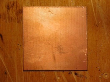
The most common available materials for the manufacture of circuit boards - these are Getinax and Fiberglass. Getinax paper impregnated with bakelite varnish, fiberglass textolite with epoxy. We will definitely use fiberglass!
Foil fiberglass laminate is sheets made from glass fabrics impregnated with a binder based on epoxy resins and lined on both sides with copper electrolytic galvanic resistant foil 35 microns thick. Extremely permissible temperature from -60ºС to +105ºС. It has very high mechanical and electrical insulating properties, and lends itself well to machining cutting, drilling, stamping.
Fiberglass is mainly used single or double-sided with a thickness of 1.5 mm and with copper foil with a thickness of 35 microns or 18 microns. We will use one-sided fiberglass laminate with a thickness of 0.8 mm with a foil with a thickness of 35 microns (why will be discussed in detail below).

Methods for making printed circuit boards at home
Boards can be produced chemically and mechanically.
With the chemical method, in those places where there should be tracks (pattern) on the board, a protective composition (varnish, toner, paint, etc.) is applied to the foil. Next, the board is immersed in a special solution (ferric chloride, hydrogen peroxide and others) which “corrodes” the copper foil, but does not affect the protective composition. As a result, copper remains under the protective composition. Protective composition it is subsequently removed with a solvent and the finished board remains.
At mechanical method a scalpel is used (for hand made) or milling machine. A special cutter makes grooves on the foil, ultimately leaving islands with foil - the necessary pattern.
Milling machines are quite expensive, and the milling machines themselves are expensive and have a short resource. So we won't use this method.

Simplest chemical method- manual. Using a risograph varnish, we draw tracks on the board and then etch them with a solution. This method does not allow making complex boards with very thin traces - so this is not our case either.

The next method of making circuit boards is using photoresist. This is a very common technology (boards are made using this method at the factory) and is often used at home. There are a lot of articles and methods for making boards using this technology on the Internet. It gives very good and repeatable results. However, this is also not our option. The main reason is quite expensive materials(photoresist, which also deteriorates over time), and also additional tools(UV illumination lamp, laminator). Of course, if you have a large-scale production of circuit boards at home - then photoresist is unrivaled - we recommend mastering it. It is also worth noting that the equipment and photoresist technology allows the production of silk-screen printing and protective masks on boards.

With the advent of laser printers, radio amateurs began to actively use them for the manufacture of circuit boards. As you know, a laser printer uses “toner” to print. This is a special powder that sinteres under temperature and sticks to the paper - the result is a drawing. The toner is resistant to various chemicals, this allows it to be used as a protective coating on the surface of copper.
So, our method is to transfer toner from paper to the surface of copper foil and then etch the board with a special solution to create a pattern.
Due to its ease of use, this method has become very widespread in amateur radio. If you type in Yandex or Google how to transfer toner from paper to a board, you will immediately find a term such as “LUT” - laser ironing technology. Boards using this technology are made like this: the pattern of the tracks is printed in a mirror version, the paper is applied to the board with the pattern on the copper, the top of this paper is ironed, the toner softens and sticks to the board. The paper is then soaked in water and the board is ready.

There are “a million” articles on the Internet about how to make a board using this technology. But this technology has many disadvantages that require direct hands and a very long time to adapt yourself to it. That is, you need to feel it. The payments don't come out the first time, they come out every other time. There are many improvements - using a laminator (with modification - the usual one does not have enough temperature), which allows you to achieve very good results. There are even methods for constructing special heat presses, but all this again requires special equipment. The main disadvantages of LUT technology:
overheating - the tracks spread out - become wider
underheating - the tracks remain on the paper
the paper is “fried” to the board - even when wet it is difficult to come off - as a result, the toner may be damaged. There is a lot of information on the Internet about what paper to choose.
Porous toner - after removing the paper, micropores remain in the toner - through them the board is also etched - corroded tracks are obtained
repeatability of the result - excellent today, bad tomorrow, then good - it is very difficult to achieve a stable result - you need a strictly constant temperature for warming up the toner, you need stable contact pressure on the board.
By the way, I was unable to make a board using this method. I tried to do it both on magazines and on coated paper. As a result, I even spoiled the boards - the copper swelled due to overheating.
For some reason, there is unfairly little information on the Internet about another method of toner transfer - the cold chemical transfer method. It is based on the fact that toner is not soluble in alcohol, but is soluble in acetone. As a result, if you choose a mixture of acetone and alcohol that will only soften the toner, then it can be “re-glued” onto the board from paper. I really liked this method and immediately bore fruit - the first board was ready. However, as it turned out later, I could not find detailed information anywhere that would give 100% results. We need a method that even a child could make the board with. But the second time it didn’t work out to make the board, then again it took a long time to select the necessary ingredients.
As a result, after much effort, a sequence of actions was developed, all components were selected that give, if not 100%, then 95% of a good result. And most importantly, the process is so simple that the child can make the board completely independently. This is the method we will use. (of course, you can continue to bring it to the ideal - if you do better, then write). The advantages of this method:
all reagents are inexpensive, accessible and safe
no additional tools needed (irons, lamps, laminators - nothing, although not - you need a saucepan)
there is no way to damage the board - the board does not heat up at all
the paper comes off on its own - you can see the result of the toner transfer - where the transfer did not come out
there are no pores in the toner (they are sealed with paper) - therefore, there are no mordants
we do 1-2-3-4-5 and we always get the same result - almost 100% repeatability
Before we start, let's see what boards we need and what we can do at home using this method.
Basic requirements for manufactured boards
We will make devices on microcontrollers, using modern sensors and microcircuits. Microchips are getting smaller and smaller. Accordingly, the following requirements for boards must be met:
the boards must be double-sided (as a rule, it is very difficult to wire a single-sided board, making four-layer boards at home is quite difficult, microcontrollers need a ground layer to protect against interference)
the tracks should be 0.2mm thick - this size is quite enough - 0.1mm would be even better - but there is a possibility of etching and the tracks coming off during soldering
the gaps between tracks are 0.2mm - this is enough for almost all circuits. Reducing the gap to 0.1mm is fraught with merging of tracks and difficulty in monitoring the board for short circuits.
We will not use protective masks, nor will we do silk-screen printing - this will complicate production, and if you are making the board for yourself, then there is no need for this. Again, there is a lot of information on this topic on the Internet, and if you wish, you can organize the “marathon” yourself.
We will not tin the boards, this is also not necessary (unless you are making a device for 100 years). For protection we will use varnish. Our main goal is to quickly, efficiently, and cheaply make a board for the device at home.
This is what the finished board looks like. made by our method - tracks 0.25 and 0.3, distances 0.2

How to make a double-sided board from 2 single-sided ones
One of the challenges of making double-sided boards is aligning the sides so that the vias line up. Usually a “sandwich” is made for this. Two sides are printed on a sheet of paper at once. The sheet is folded in half, and the sides are accurately aligned using special marks. Double-sided textolite is placed inside. With the LUT method, such a sandwich is ironed and a double-sided board is obtained.
However, with the cold toner transfer method, the transfer itself is carried out using a liquid. And therefore it is very difficult to organize the process of wetting one side at the same time as the other side. This, of course, can also be done, but with the help special device- mini press (vice). Thick sheets of paper are taken - which absorb the liquid to transfer toner. The sheets are wetted so that the liquid does not drip and the sheet holds its shape. And then a “sandwich” is made - a moistened sheet, a sheet toilet paper to absorb excess liquid, a sheet with a pattern, a double-sided board, a sheet with a pattern, a sheet of toilet paper, again a dampened sheet. All this is clamped vertically in a vice. But we won’t do that, we’ll do it simpler.
A very good idea came up on board manufacturing forums - what a problem it is to make a double-sided board - take a knife and cut the PCB in half. Since fiberglass is a layered material, this is not difficult to do with a certain skill:

As a result, from one double-sided board with a thickness of 1.5 mm we get two single-sided halves.

Next we make two boards, drill them and that’s it - they are perfectly aligned. It was not always possible to cut the PCB evenly, and in the end the idea came to use a thin one-sided PCB with a thickness of 0.8 mm. The two halves do not need to be glued together; they will be held together by soldered jumpers in the vias, buttons, and connectors. But if necessary, you can glue it with epoxy glue without any problems.
The main advantages of this hike:
Textolite with a thickness of 0.8 mm is easy to cut with paper scissors! In any shape, that is, it is very easy to cut to fit the body.
Thin PCB - transparent - by shining a flashlight from below you can easily check the correctness of all tracks, short circuits, breaks.
Soldering one side is easier - the components on the other side do not interfere and you can easily control the soldering of the microcircuit pins - you can connect the sides at the very end
You need to drill twice as many holes and the holes may slightly mismatch
The rigidity of the structure is slightly lost if you do not glue the boards together, but gluing is not very convenient
Single-sided fiberglass laminate with a thickness of 0.8mm is difficult to buy; most people sell 1.5mm, but if you can’t get it, you can cut thicker textolite with a knife.
Let's move on to the details.
Required Tools and chemistry
We will need the following ingredients:


Now that we have all this, let’s take it step by step.
1. Layout of board layers on a sheet of paper for printing using InkScape

Automatic collet set:

We recommend the first option - it is cheaper. Next, you need to solder wires and a switch (preferably a button) to the motor. It is better to place the button on the body to make it more convenient to quickly turn the motor on and off. All that remains is to choose a power supply, you can take any power supply with 7-12V current 1A (less is possible), if there is no such power supply, then USB charging at 1-2A or a Krona battery may be suitable (you just have to try it - not everyone likes charging motors, the motor may not start).
The drill is ready, you can drill. But you just need to drill strictly at an angle of 90 degrees. You can build a mini machine - there are various schemes on the Internet:

But there is a simpler solution.
Drilling jig
To drill exactly 90 degrees, it is enough to make a drilling jig. We will do something like this:

It is very easy to make. Take a square of any plastic. We place our drill on a table or other flat surface. And drill a hole in the plastic using the required drill. It is important to ensure an even horizontal movement of the drill. You can lean the motor against the wall or rail and the plastic too. Next, use a large drill to drill a hole for the collet. WITH reverse side drill or cut a piece of plastic so that the drill is visible. You can glue a non-slip surface to the bottom - paper or rubber band. Such a jig must be made for each drill. This will ensure perfectly accurate drilling!
This option is also suitable, cut off part of the plastic on top and cut off a corner from the bottom.

Here's how to drill with it:

We clamp the drill so that it sticks out 2-3mm when the collet is fully immersed. We put the drill in the place where we need to drill (when etching the board, we will have a mark where to drill in the form of a mini hole in the copper - in Kicad we specially put a checkmark for this, so that the drill will stand there on its own), press the jig and turn on the motor - hole ready. For illumination, you can use a flashlight by placing it on the table.
As we wrote earlier, you can only drill holes on one side - where the tracks fit - the second half can be drilled without a jig along the first guide hole. This saves a little effort.
8. Tinning the board
Why tin the boards - mainly to protect copper from corrosion. The main disadvantage of tinning is overheating of the board and possible damage to the tracks. If you don’t have a soldering station, definitely don’t tin the board! If it is, then the risk is minimal.
You can tin a board with ROSE alloy in boiling water, but it is expensive and difficult to obtain. It is better to tin with ordinary solder. To do this efficiently, you need to make a simple device with a very thin layer. We take a piece of braid for soldering parts and put it on the tip, screw it to the tip with wire so that it does not come off:
We cover the board with flux - for example LTI120 and the braid too. Now we put tin into the braid and move it along the board (paint it) - we get an excellent result. But as you use the braid, it comes apart and copper fluff begins to remain on the board - they must be removed, otherwise there will be a short circuit! You can see this very easily by shining a flashlight on the back of the board. With this method, it is good to use either a powerful soldering iron (60 watt) or ROSE alloy.
As a result, it is better not to tin the boards, but to varnish them at the very end - for example, PLASTIC 70, or simple acrylic varnish purchased from auto parts KU-9004:

Fine tuning of the toner transfer method
There are two points in the method that can be tuned and may not work right away. To configure them, you need to make a test board in Kicad, tracks in a square spiral of different thicknesses, from 0.3 to 0.1 mm and with different intervals, from 0.3 to 0.1 mm. It is better to immediately print several such samples on one sheet and make adjustments.
Possible problems that we will fix:
1) tracks can change geometry - spread out, become wider, usually very little, up to 0.1mm - but this is not good
2) the toner may not stick well to the board, come off when the paper is removed, or stick poorly to the board
The first and second problems are interconnected. I solve the first one, you come to the second one. We need to find a compromise.
The tracks can spread for two reasons - too much pressure, too much acetone in the resulting liquid. First of all, you need to try to reduce the load. The minimum load is about 800g, it is not worth reducing below. Accordingly, we place the load without any pressure - we just put it on top and that’s it. There must be 2-3 layers of toilet paper to ensure good absorption of excess solution. You must ensure that after removing the weight, the paper should be white, without purple smudges. Such smudges indicate severe melting of the toner. If you can’t adjust it with a weight and the tracks still blur, then increase the proportion of nail polish remover in the solution. You can increase to 3 parts liquid and 1 part acetone.
The second problem, if there is no violation of the geometry, indicates insufficient weight of the load or a small amount of acetone. Again, it’s worth starting with the load. More than 3 kg does not make sense. If the toner still does not stick well to the board, then you need to increase the amount of acetone.
This problem mainly occurs when you change your nail polish remover. Unfortunately, this is not a permanent or pure component, but it was not possible to replace it with another. I tried to replace it with alcohol, but apparently the mixture is not homogeneous and the toner sticks in some patches. Also, nail polish remover may contain acetone, then less of it will be needed. In general, you will need to carry out such tuning once until the liquid runs out.
The board is ready
If you do not immediately solder the board, it must be protected. The easiest way to do this is to coat it with alcohol rosin flux. Before soldering, this coating will need to be removed, for example, with isopropyl alcohol.
Alternative options
You can also make a board:
Additionally, custom board manufacturing services are now gaining popularity - for example Easy EDA. If you need a more complex board (for example, a 4-layer board), then this is the only way out.
A printed circuit board is a dielectric plate on the surface of which conductive tracks are applied and places are prepared for mounting electronic components. Electrical radio components are usually installed on the board using soldering.
PCB device
The electrically conductive paths of the board are made of foil. The thickness of the conductors is, as a rule, 18 or 35 microns, less often 70, 105, 140 microns. The board has holes and contact pads for mounting radio elements.
Separate holes are used to connect conductors located on different sides of the board. A special protective coating and markings are applied to the outer sides of the board.
Stages of creating a printed circuit board
In amateur radio practice, one often has to deal with the development, creation and manufacture of various electronic devices. Moreover, any device can be built on a printed circuit board or a regular board with wall-mounted. The PCB works much better, is more reliable and looks more attractive. Creating it involves performing a number of operations:
Preparation of the layout;
Drawing on textolite;
Etching;
Tinning;
Installation of radio elements.

Manufacturing printed circuit boards is a complex, labor-intensive, and interesting process.
Development and production of a layout
The board drawing can be done manually or on a computer using one of the special programs.
It is best to draw the board manually on recorder paper on a 1:1 scale. Graph paper is also suitable. Installed electronic components must be displayed in mirror image. The tracks on one side of the board are shown as solid lines, and on the other side as dotted lines. The dots mark the places where radio elements are attached. Soldering areas are drawn around these places. All drawings are usually made using a drawing board. Typically done manually simple drawings, more complex circuits printed circuit boards are developed on a computer in special applications.

Most often they use a simple program called Sprint Layout. Only a laser printer is suitable for printing. The paper should be glossy. The main thing is that the toner does not eat into it, but remains on top. The printer must be adjusted so that the toner thickness of the drawing is maximum.
Industrial production of printed circuit boards begins with entering the circuit diagram of the device into a computer-aided design system, which creates a drawing of the future board.
Preparing the workpiece and drilling holes
First of all, you need to cut a piece of PCB with the given dimensions. File the edges. Attach the drawing to the board. Prepare the tool for drilling. Drill directly according to the drawing. The drill must be good quality and correspond to the diameter of the smallest hole. If possible, you should use a drilling machine.

Having made all the necessary holes, remove the drawing and drill each hole to the specified diameter. Clean the surface of the board with fine sandpaper. This is necessary to eliminate burrs and improve paint adhesion to the board. To remove traces of grease, treat the board with alcohol.
Drawing on fiberglass laminate
The board drawing can be applied to the PCB manually or using one of many technologies. Laser ironing technology is the most popular.
Manual drawing begins by marking the mounting areas around the holes. They are applied using a drawing pen or a match. The holes are connected with tracks in accordance with the drawing. It is better to draw with nitro paint in which rosin is dissolved. This solution provides strong adhesion to the board and good resistance to etching with high temperature. Asphalt bitumen varnish can be used as paint.
Manufacturing printed circuit boards using laser-iron technology gives good results. It is important to perform all operations correctly and carefully. The degreased board must be placed on a flat surface with the copper facing up. Carefully place the design on top with the toner facing down. Additionally, add a few more sheets of paper. Iron the resulting structure with a hot iron for about 30-40 seconds. When exposed to temperature, the toner should change from a solid to a viscous state, but not to a liquid. Let the board cool and place it in warm water for a few minutes.

The paper will become limp and tear off easily. You should carefully examine the resulting drawing. The absence of separate tracks indicates that the iron temperature is insufficient; wide tracks are obtained when the iron is too hot or the board is heated for an excessively long time.
Small defects can be corrected with a marker, paint or nail polish. If you don’t like the workpiece, then you need to wash everything off with a solvent, clean it with sandpaper and repeat the process again.
Etching
A grease-free printed circuit board is placed in a plastic container with the solution. At home, ferric chloride is usually used as a solution. The bath with it needs to be rocked periodically. After 25-30 minutes, the copper will completely dissolve. Etching can be accelerated by using a heated ferric chloride solution. At the end of the process, the printed circuit board is removed from the bath and thoroughly washed with water. Then the paint is removed from the conductive paths.
Tinning
There are many methods of tinning. We have a prepared printed circuit board. At home, as a rule, there are no special devices and alloys. Therefore, they use a simple, reliable method. The board is coated with flux and tinned with a soldering iron with regular solder using copper braiding.
Installation of radio elements
At the final stage, the radio components are inserted one by one into the places intended for them and soldered. Before soldering, the legs of the parts must be treated with flux and, if necessary, shortened.

The soldering iron should be used carefully: if there is excess heat, the copper foil may begin to peel off and the printed circuit board will be damaged. Remove any remaining rosin with alcohol or acetone. The finished board can be varnished.
Industrial development
It is impossible to design and manufacture a printed circuit board for high-end equipment at home. For example, the printed circuit board of an amplifier for High-End equipment is multi-layered, copper conductors are coated with gold and palladium, conductive tracks have different thicknesses, etc. Achieving this level of technology is not easy even in an industrial enterprise. Therefore, in some cases it is advisable to purchase a ready-made high-quality board or place an order to carry out work according to your own scheme. Currently, the production of printed circuit boards is established at many domestic enterprises and abroad.